1. 通过较强的金属二维材料面外作用力来精准操控二维材料层间转角并固定角度
北京大学刘开辉,上海科技大学王竹君等,Nature Materials,21 1263-1268(2022)
doi.org/10.1038/s41563-022-01361-8
大规模制备角度可控的大面积扭曲双层石墨烯(TBG)是其应用的先决条件。然而,目前大多数制造扭曲双层石墨烯的策略都面临着巨大的挑战,其中转移方法很容易受到界面污染的阻碍,而直接生长方法则缺乏扭曲角度设计的灵活性。在这里,北大刘开辉和上海科技大学王竹君课题组开发了一种有效的策略,可以生长出具有任意扭曲角度(精确度小于 1.0°)的厘米级 TBG。通过从两个预旋转的单晶 Cu(111) 箔复制角度,形成 Cu/TBG/Cu 夹层结构,并通过定制开发的等电位表面蚀刻工艺将 TBG 从该结构中分离出来,成功实现了精确的角度控制。光学光谱、电子显微镜、光发射光谱和光电流光谱等综合表征技术清楚地说明了扭转角的准确性和一致性。该工作为设计生长大规模二维扭曲双层膜开辟了一条便捷的途径,从而为未来在集成层面应用扭曲电子学奠定了物质基础。

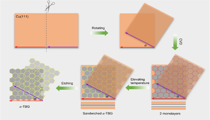
制备工艺:将一块单晶铜(111)箔切成边缘平行的两块(红色和紫色标记)。然后,在两个标记的边缘之间以旋转角度 α 叠放这两块铜箔。然后,通过 CVD 方法在两个相邻的铜(111)表面之间外延生长石墨烯。随后,通过将铜加热到高温,得到了具有扭曲角 α 的双层石墨烯,最后在蚀刻掉铜后将其分离出来.

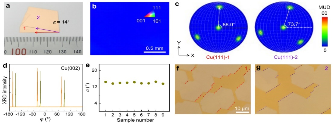
Fig.2 Photograph of two stacked Cu foils with rotation angle α. The numbers on the ruler indicate the length in millimetres. b, EBSD IPF map of the Cu foil. The uniform blue colour reveals the single-crystal structure of the (111) facet index. c, EBSD PFs of the two Cu pieces, marked as Cu(111)-1 and Cu(111)-2. The multiples of uniform density (MUD) results present a relative rotation angle of 14.3°. d, XRD φ-scan data for Cu(111)-1 (orange curve) and Cu(111)-2 (dark yellow curve) obtained by fixing along the Cu(002) direction. The three-fold symmetry of diffraction peaks indicates the high crystallinity and a shift of 14.2° between the two spectra. e, Statistical data of the rotation angles for nine stacked Cu foils measured by EBSD, indicating the small deviation of ~1.0°. f,g, Optical images of the hexagonal graphene domains on the top surfaces of Cu(111)-1 (f) and Cu(111)-2 (g), with a relative rotation angle of ~14°.

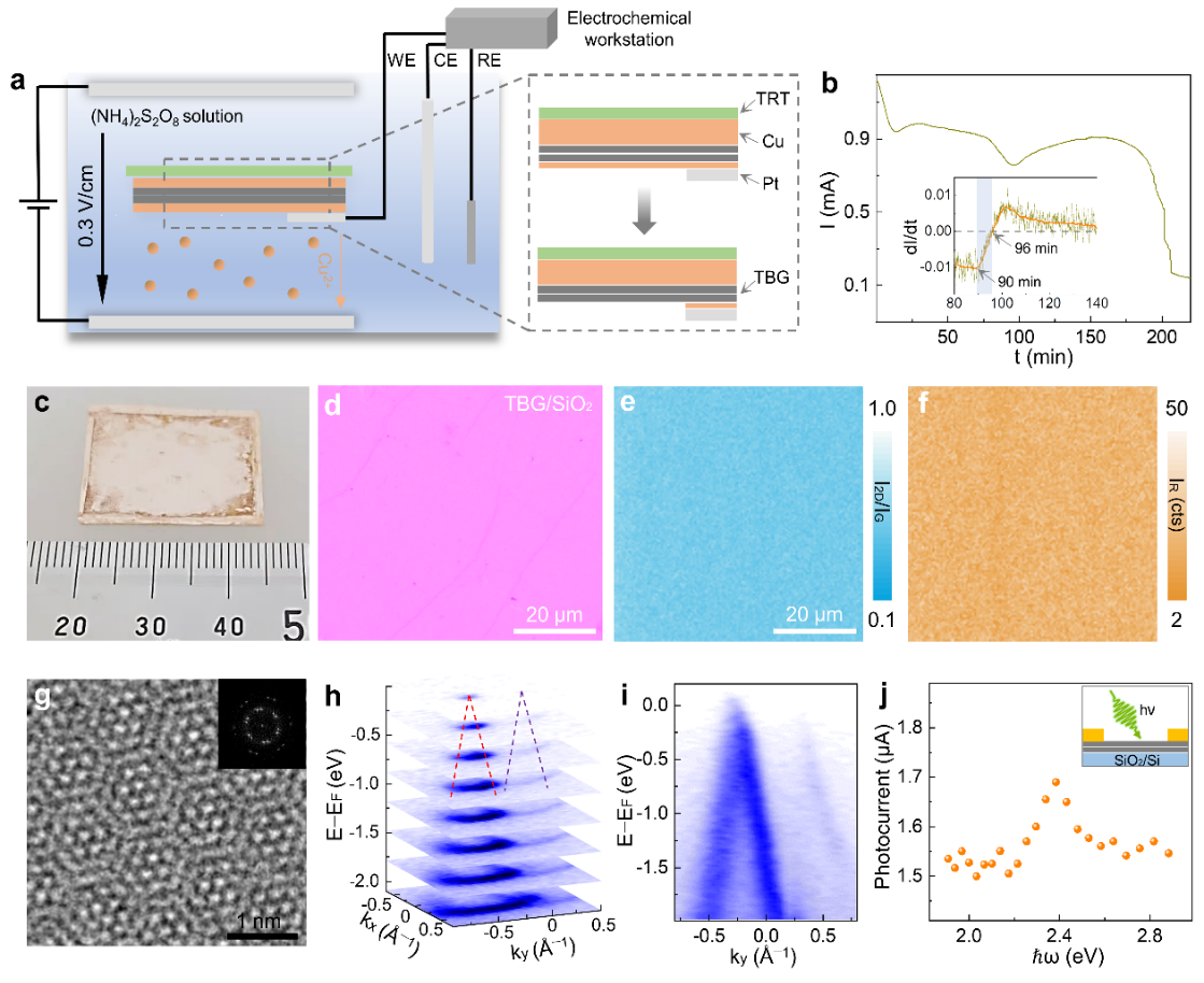
Fig.3 a, Schematic of the equipotential surface etching process. TBG was obtained by etching one side of the Cu(111) foil with the other side protected by TRT. The three-electrode system consists of a working electrode (WE), reference electrode (RE) and counter electrode (CE). b, Time (t) evolution of current (I) during the etching process. The inset shows the time evolution of the derivative of current during the etching process. c, Photograph of the Cu(111) foil with a freshly exposed bilayer graphene film. The numbers on the ruler indicate the length in millimetres. d, Optical image of bilayer graphene after transferring onto the SiO2/Si substrate. e,f, Raman mappings of I2D/IG and IR, verifying the uniformity of the obtained bilayer graphene film. g, HRTEM image of bilayer graphene. The inset shows the fast Fourier transform pattern of the HRTEM image. h, Stacking plot of constant-energy contours at different binding energies in kx–ky plane of the bilayer graphene. i, ARPES spectrum of the bilayer graphene across the two adjacent Dirac cones of h along the ky direction. j, Photocurrent versus the photon energy (ħω) of incident light. These results prove that the twist angle of bilayer graphene is ~14°.
2. 由量子自旋霍尔层构建的过渡金属二氯化物的拓扑层次结构的研究
上海科技大学陈宇林,柳仲楷,清华大学何珂等
Advanced Materials, 2300227, (2023) doi.org/10.1002/adma.202300227
二维材料的物理特性从单层的极限到块体的演变揭示了尺寸效应的独特特性,并为其应用提供了新颖的调制手段。单层1T'相过渡金属二氯化物(1T'-TMD)具有无处不在的量子自旋霍尔态,是三维拓扑相的理想二维构件。然而,堆积的几何形状以前只限于1T‘-WTe2类型。由于平移堆叠的1T’-单层组成的新型2M-TMD被认为具有可调控的倒带隙和层间耦合潜在材料单元。通过对2M-TMD的电子结构进行偏振依赖性的ARPES以及第一原理计算,揭示了拓扑层次:2M-WSe2、MoS2和MoSe2是弱拓扑绝缘体(WTIs),而2M-WS2是强拓扑绝缘体(STI)。通过调整层间距离进一步证明拓扑相变,表明带状反转幅度和层间耦合共同决定了2M-TMD的不同拓扑状态。研究表明,2M-TMDs是包括拓扑超导体在内的各种奇异相的母体化合物,由于其与二维材料的灵活图案设计,在量子电子学方面有很大的应用潜力。

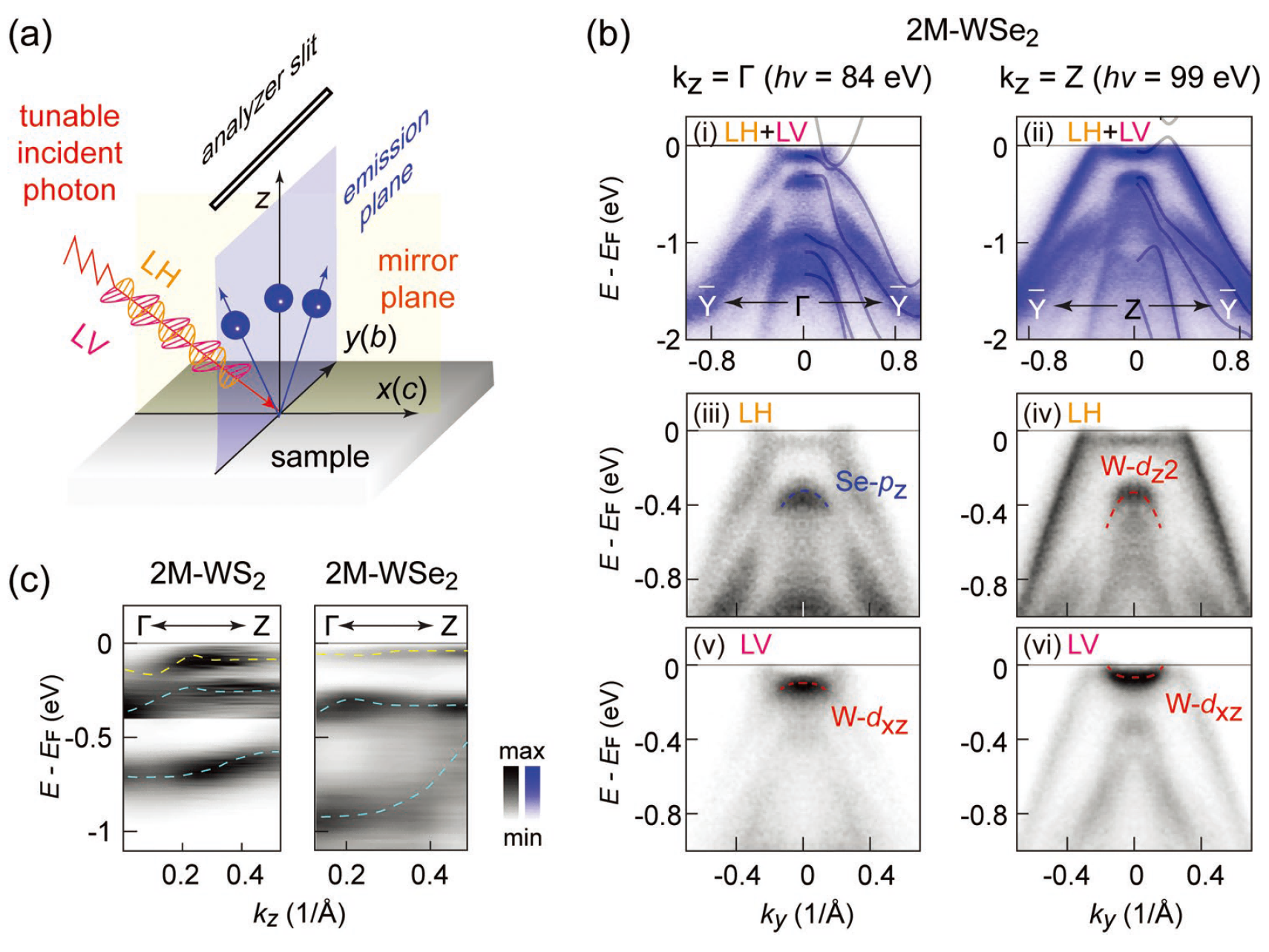
Fig.4 Photon-energy- and polarization-dependent angle-resolved photoemission spectroscopy (ARPES) measurements. a) Schematic polarization geometry used in the ARPES experiment, where the linear horizontal (LH) and linear vertical (LV)-polarized light are incident on the sample parallel and perpendicular with respect to the detection plane (xz-plane). b)(i) and (ii) Polarization-integrated ARPES results of 2M-WSe2 dispersion along (i) 𝑌¯−𝛤−𝑌¯ with a photon energy of 84 eV and (ii) 𝑌¯−𝑍−𝑌¯ with a photon energy of 99 eV. The corresponding calculation is appended. (iii)-(vi) Polarization-dependent ARPES results of 2M-WSe2 dispersion along 𝑌¯−𝛤−𝑌¯ and 𝑌¯−𝑍−𝑌¯ near EF. ARPES results are symmetrized with respect to ky = 0 based on the crystalline symmetry. Blue and red dashed lines are guides to the eyes, which indicate the bands mainly contributed by specific Se and W orbitals, respectively. See more details in Note S3 and S10 (Supporting Information). c) Photon-energy-dependent ARPES measurements on the kz dispersion of 2M-WS2 and 2M-WSe2. The yellow and cyan dashed lines representing the three topmost valence bands are guides to the eyes.
Nano-ARPES测试结果及细节
附件下载:
